
Metasurfaces and Nanoscale Optics
Metasurfaces and Nanoscale Optics
Precision compact optics including metalenses, waveguide gratings, and diffractive optical elements will be integral to enabling fully immersive AR/VR experiences, next generation medical imaging, advanced terrain mapping and other emerging technologies. The key to widespread adaptation will be the availability of scalable fabrication methods that enable precise control over the dimensions and placement of nanoscale features with high aspect ratios, high refractive index (RI) and excellent long-term stability. Utilizing novel nanoparticle dispersion inks in combination with nanoimprint lithography, we have developed a method for high throughput manufacturing of large quantities of all-inorganic metalenses (fig. 1), diffraction elements (fig. 2), waveguide gratings and other optical elements. These components are “printed” in a single step with process times under two minutes. By controlling the process from material selection to final device verification, we can achieve critical dimension adjustments to consistently improve device design and quality.
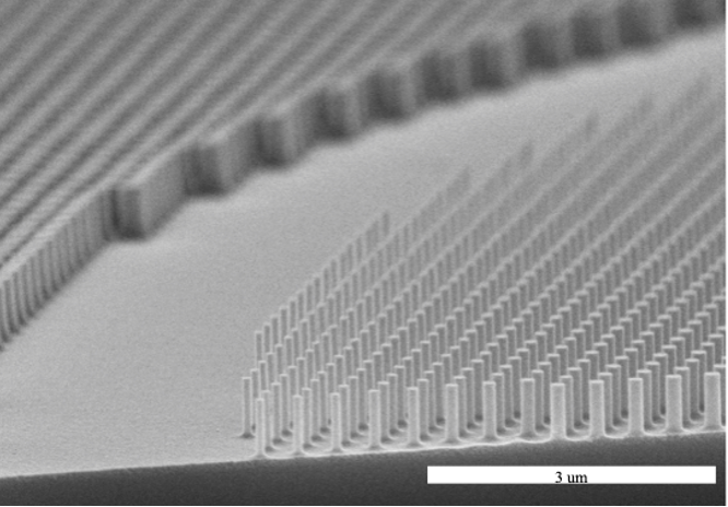
Figure 1. Cross sectional SEM image of high RI pillars arranged for a convergent metalens
Our baseline process yields a RI of 1.9, lenses with critical dimensions below 60 nm, feature aspect ratios greater than 8. In our first report we achieved efficiencies greater than 55% and consistent device performance across 15 lenses printed within 30 minutes (Figure 4).1 Recent improvements have pushed efficiencies beyond 65 %.
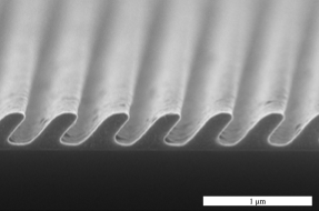
Figure 2. SEM image of high RI slanted diffraction gratings. Master from NIL Technologies.
We use a simple post imprint ALD process to tune RI from 1.9 up to 2.2. The increase in RI can be used to increase the efficiencies of the lenses, increase accessible field of view in AR/VR applications and, when desired, tune the RI of the imprinted components to match the substrate, which eliminates the need to control residual layer thickness. ALD tuning to RI=2.2 requires less than 25 cycles, so the incremental cost of this step is quite small.
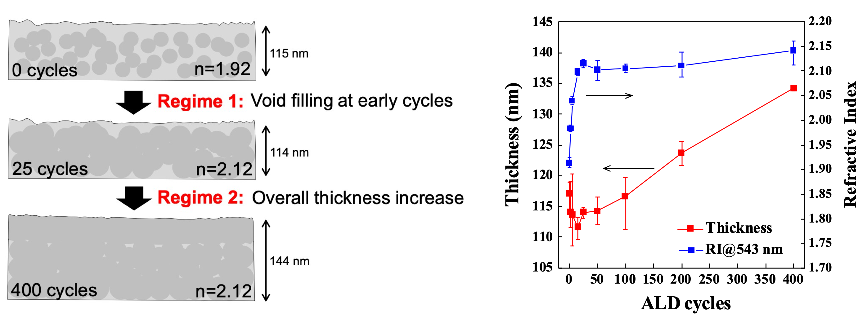
Figure 3. RI tuning of inorganic composite films from 1.9 to 2.1 showing two regimes, one where the RI increases without increasing the film thickness (void filling) and one where the film thickness increases without increasing RI (cladding).
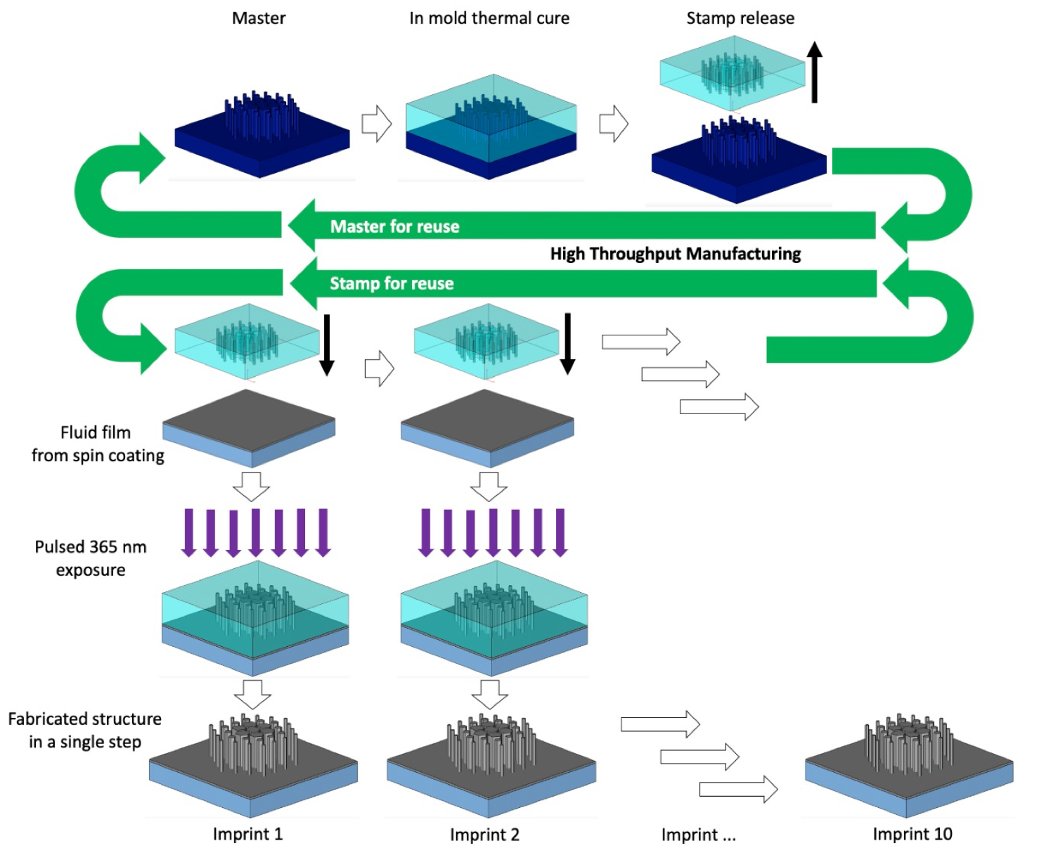
Figure 4. Process flow for the fabrication of metalenses with a 2-minute cycle time (30 wafers/hr), showing stamp making from the silicon master (top) and imprint series with spin coated films, UV curing and the same elastomeric stamp throughout (bottom).
Optical, environmental and thermal stability are required for commercial products but have been quite difficult to achieve using imprinted polymer or polymer/nanoparticle composite materials. Our process yields all-inorganic TiO2 devices with exceptional stability to accelerated weathering, high temperature, humidity, and thermal cycling. Figure 5 shows the stability of our 2.0, 2.1 and 2.2 RI materials compared to a typical TiO2 nanoparticle polymer composite after the equivalent exposure to 1 year of Florida weather and a 480-hour high temperature (80oC), high humidity (85%) soak followed by 45 thermal cycles between -20oC and 80oC. The printed all-inorganic samples are stable while the TiO2 nanoparticle polymer composite exhibits a severe increase in haze as well as dimensional and optical instability.
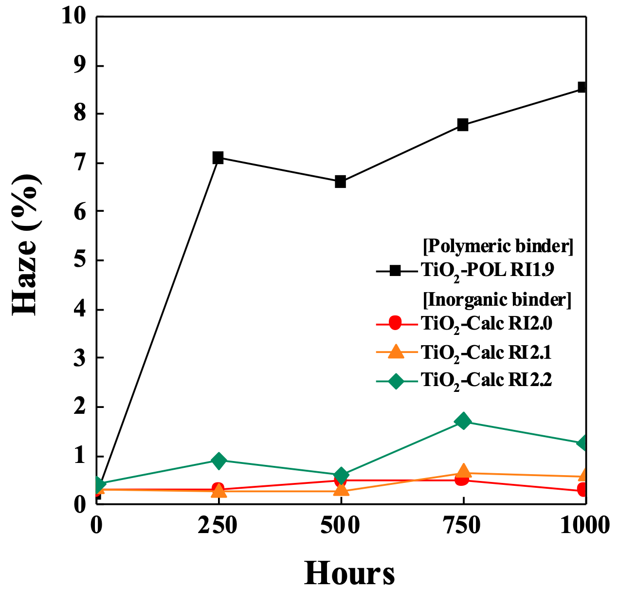
Figure 5. Averaged values of haze obtained over the visible range from 400 to 800 nm from accelerated weathering testing conducted by Applied Technical Services.
The homogeneity of the all-inorganic nanocrystal composites films and imprinted devices is evident using focus-ion beam transmission electron microscopy (FIB TEM). Three films consisting of nanocrystal TiO2 composites calcined at 500ºC with 0, 15 and 400 cycles of ALD were characterized to visualize the homogeneity of ALD deposited TiO2 into the composite (backfilling) and onto the composite surface (cladding). The FIB TEM images in figure 6 show homogeneity of the small crystalline nanoparticles confirmed by diffraction patterns and absence voids. The backfilled sample with 15 cycles of ALD show no evidence of cladding despite an increase in RI to 2.2. The sample treated with 400 cycles of ALD shows a cladding layer with a clear boundary with the backfilled NP film. Crystallinity in the ALD cladded layer is due to the high deposition temperature, yielding anatase TiO2 growth. The imprinted all-inorganic composite demonstrates the packing uniformity of the nanocrystals throughout the imprinted structure. The tops of the features are embedded in the FIB lamella, showing contrast due to the conductive coating. Optical homogeneity is also evident in the VASE analysis of the backfilled films, which shows excellent fit to a single layer Cauchy model with low MSE (Figure 3).
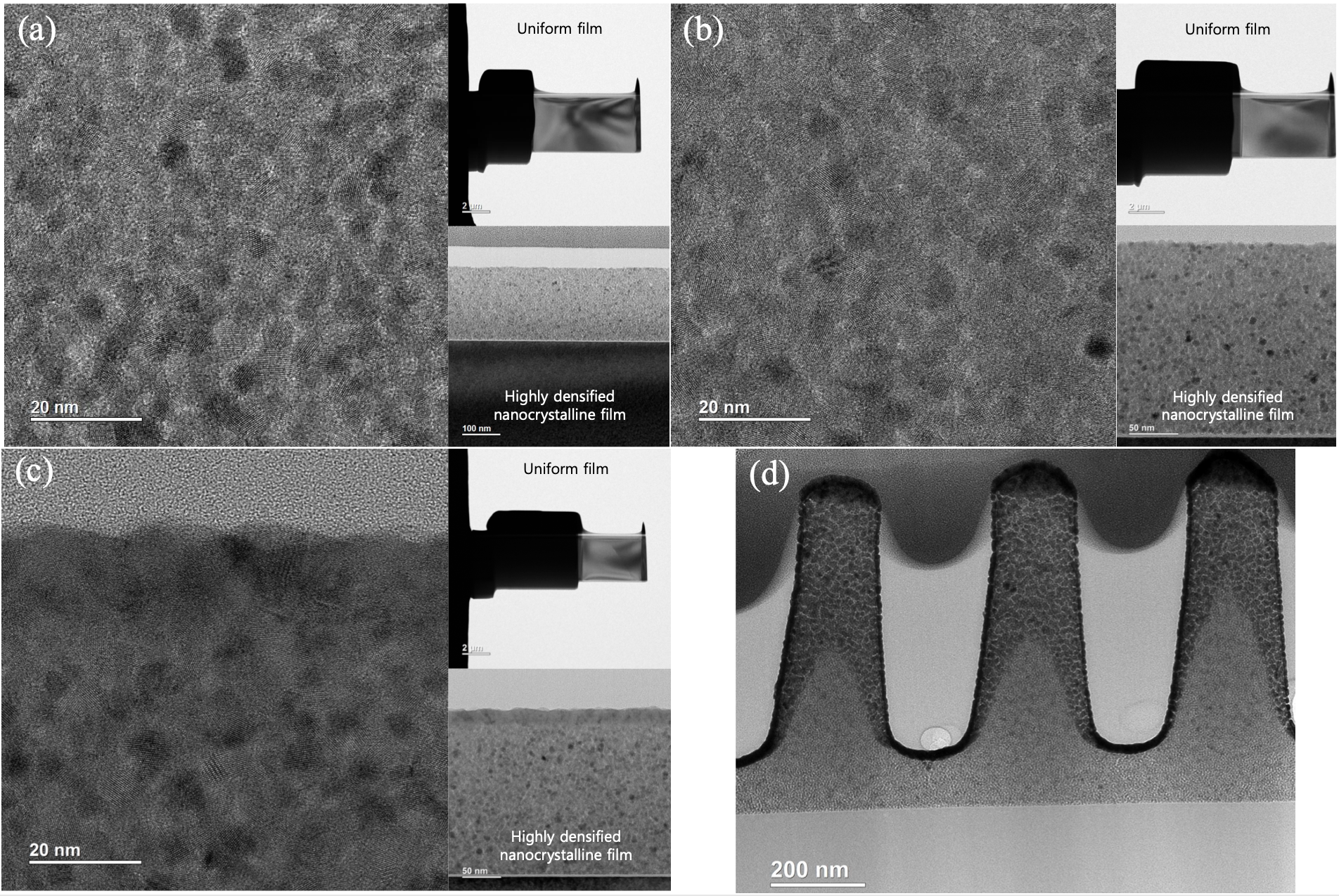
Figure 6. FIB TEM images of nanocrystal TiO2 composite calcined at 500ºC with 0 (a), 15 (b) and 400 (c) cycles of ALD and a metalens imprint from the same formulation and 0 cycles of ALD (d).
We have fabricated 300 mm full wafer master wafer containing over 2,000 individual metalenses (Figure 7) and imprint trials are underway. With imprint cycle times on the order of 2 minutes, >30,000 metalenses can be fabricated in half an hour on a single tool. High throughput production drastically opens up the potential for nanoscale optics to reach their desired markets.
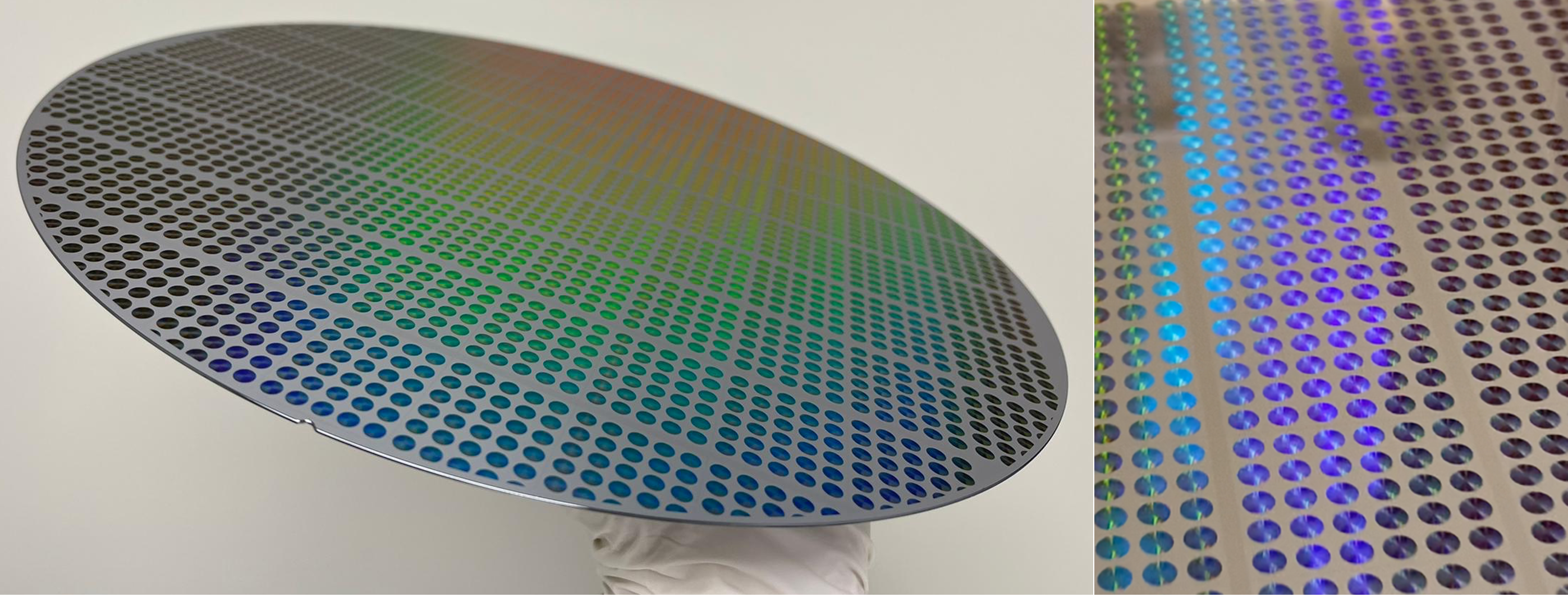
Figure 7. 300 mm silicon metalens master containing 2,350 discrete 4 mm lenses for 543 nm wavelength operation.
Related publications:
1. Einck VJ, Torfeh M, McClung A, Jung DE, Mansouree M, Arbabi A, Watkins JJ. “Scalable Nanoimprint Lithography Process for Manufacturing Visible Metasurfaces Composed of High Aspect Ratio TiO2 Meta-Atoms”. ACS Photonics 2021, 8(8) 2400-2409.
2. Cates, Nichole, Vincent Einck, Lauren Micklow, Jacobo Morère, Uzodinma Okoroanyanwu, James J. Watkins, and Stephen Furst. "Roll-to-roll nanoimprint lithography using a seamless cylindrical mold nanopatterned with a high-speed mastering process". Nanotechnology 2021, 32(15) 155301.
3. Irene R. Howell, Vincent J. Einck, Dieter Nees, Barbara Stadlober, James J. Watkins. "Solvent-Free, Transparent, High-Refractive Index ZrO2 Nanoparticle Composite Resin for Scalable Roll to Roll UV-Nanoimprint Lithography". Optics & Laser Technology 2021, 140, 107101.
4. Arisoy, Feyza Dundar, Ilja Czolkos, Alicia Johansson, Theodor Nielsen, and James J. Watkins. "Low-cost, durable master molds for thermal-NIL, UV-NIL, and injection molding". Nanotechnology 2019 31(1) 015302.
5. Howell IR, Giroire B, Garcia A, Li S, Aymonier C, Watkins JJ. "Fabrication of plasmonic TiN nanostructures by nitridation of nanoimprinted TiO 2 nanoparticles". Journal of Materials Chemistry C 2018 6(6),1399-1406.
6. Li S, Kazemi-Moridani A, Zhou Y, Howell I.R, Kothari R, Lee JH, Watkins JJ. “Wavelength-Selective Three-Dimensional Thermal Emitters via Imprint Lithography and Conformal Metallization”. ACS applied materials & interfaces 2018, 10(9), 8173-8179.
7. Kothari R, Beaulieu MR, Hendricks NR, Li S and Watkins JJ. “Direct Patterning of Robust One-Dimensional, Two-Dimensional, and Three-Dimensional Crystalline Metal Oxide Nanostructures Using Imprint Lithography and Nanoparticle Dispersion Inks”. Chemistry of Materials 2017, 29(9), 3908-3918.